- 您现在的位置:买卖IC网 > Sheet目录3850 > PIC18F86J11-I/PT (Microchip Technology)IC PIC MCU FLASH 32KX16 80TQFP
2007-2012 Microchip Technology Inc.
DS39778E-page 67
PIC18F87J11 FAMILY
6.0
MEMORY ORGANIZATION
There are two types of memory in PIC18 Flash
microcontroller devices:
Program Memory
Data RAM
As Harvard architecture devices, the data and program
memories use separate busses; this allows for
concurrent access of the two memory spaces.
Additional detailed information on the operation of the
Flash program memory is provided in Section 7.0
6.1
Program Memory Organization
PIC18 microcontrollers implement a 21-bit Program
Counter (PC) which is capable of addressing a 2-Mbyte
program memory space. Accessing a location between
the upper boundary of the physically implemented
memory and the 2-Mbyte address will return all ‘0’s (a
NOP
instruction).
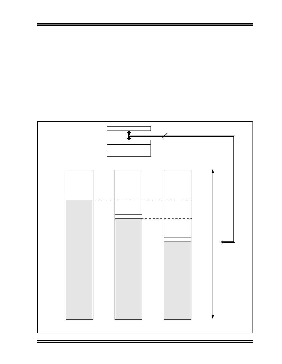
The entire PIC18F87J11 family of devices offers three
different on-chip Flash program memory sizes, from
64 Kbytes (up to 16,384 single-word instructions) to
128 Kbytes (65,536 single-word instructions). The
program memory maps for individual family members
are shown in Figure 6-3.
FIGURE 6-1:
MEMORY MAPS FOR PIC18F87J11 FAMILY DEVICES
Note:
Sizes of memory areas are not to scale. Sizes of program memory areas are enhanced to show detail.
Unimplemented
Read as ‘0’
Unimplemented
Read as ‘0’
000000h
1FFFFFF
PIC18FX6J11
PIC18FX6J16
PIC18FX7J11
00FFFFh
017FFFh
PC<20:0>
Stack Level 1
Stack Level 31
CALL, CALLW, RCALL,
RETURN, RETFIE, RETLW,
21
Us
er
M
e
mo
ry
S
pace
On-Chip
Memory
On-Chip
Memory
On-Chip
Memory
ADDULNK, SUBULNK
Config. Words
01FFFFh
Unimplemented
Read as ‘0’
发布紧急采购,3分钟左右您将得到回复。
相关PDF资料
PIC18F66J50-I/PT
IC PIC MCU FLASH 32KX16 64TQFP
PIC24FJ96GA006-I/PT
IC PIC MCU FLASH 96KB 64TQFP
PIC18F4321-I/ML
IC PIC MCU FLASH 4KX16 44QFN
PIC24FJ32GB002-I/SP
IC MCU 16BIT 32KB FLASH 28DIP
DSPIC33FJ16GP304-I/PT
IC DSPIC MCU/DSP 16K 44TQFP
PIC16C62B-20I/SP
IC MCU OTP 2KX14 PWM 28DIP
DSPIC30F2010-20I/SP
IC DSPIC MCU/DSP 12K 28DIP
AT89S52-24AC
IC MCU 8K FLASH 24MHZ 44-TQFP
相关代理商/技术参数
PIC18F86J11T-I/PT
功能描述:8位微控制器 -MCU 64KB Flash 3936bytes RAM 67 I/O RoHS:否 制造商:Silicon Labs 核心:8051 处理器系列:C8051F39x 数据总线宽度:8 bit 最大时钟频率:50 MHz 程序存储器大小:16 KB 数据 RAM 大小:1 KB 片上 ADC:Yes 工作电源电压:1.8 V to 3.6 V 工作温度范围:- 40 C to + 105 C 封装 / 箱体:QFN-20 安装风格:SMD/SMT
PIC18F86J15-I/PT
功能描述:8位微控制器 -MCU 96 KB FL 4 KB RAM RoHS:否 制造商:Silicon Labs 核心:8051 处理器系列:C8051F39x 数据总线宽度:8 bit 最大时钟频率:50 MHz 程序存储器大小:16 KB 数据 RAM 大小:1 KB 片上 ADC:Yes 工作电源电压:1.8 V to 3.6 V 工作温度范围:- 40 C to + 105 C 封装 / 箱体:QFN-20 安装风格:SMD/SMT
PIC18F86J15T-I/PT
功能描述:8位微控制器 -MCU 96 KB FL 4 KB RAM RoHS:否 制造商:Silicon Labs 核心:8051 处理器系列:C8051F39x 数据总线宽度:8 bit 最大时钟频率:50 MHz 程序存储器大小:16 KB 数据 RAM 大小:1 KB 片上 ADC:Yes 工作电源电压:1.8 V to 3.6 V 工作温度范围:- 40 C to + 105 C 封装 / 箱体:QFN-20 安装风格:SMD/SMT
PIC18F86J16-I/PT
功能描述:8位微控制器 -MCU 96KB FL 3936b RAM 10 MIPS 67 I/O RoHS:否 制造商:Silicon Labs 核心:8051 处理器系列:C8051F39x 数据总线宽度:8 bit 最大时钟频率:50 MHz 程序存储器大小:16 KB 数据 RAM 大小:1 KB 片上 ADC:Yes 工作电源电压:1.8 V to 3.6 V 工作温度范围:- 40 C to + 105 C 封装 / 箱体:QFN-20 安装风格:SMD/SMT
PIC18F86J16T-I/PT
功能描述:8位微控制器 -MCU 96KB Flash 3936bytes RAM 67 I/O RoHS:否 制造商:Silicon Labs 核心:8051 处理器系列:C8051F39x 数据总线宽度:8 bit 最大时钟频率:50 MHz 程序存储器大小:16 KB 数据 RAM 大小:1 KB 片上 ADC:Yes 工作电源电压:1.8 V to 3.6 V 工作温度范围:- 40 C to + 105 C 封装 / 箱体:QFN-20 安装风格:SMD/SMT
PIC18F86J50-I/PT
功能描述:8位微控制器 -MCU 64KB Flash 3936byte RAM RoHS:否 制造商:Silicon Labs 核心:8051 处理器系列:C8051F39x 数据总线宽度:8 bit 最大时钟频率:50 MHz 程序存储器大小:16 KB 数据 RAM 大小:1 KB 片上 ADC:Yes 工作电源电压:1.8 V to 3.6 V 工作温度范围:- 40 C to + 105 C 封装 / 箱体:QFN-20 安装风格:SMD/SMT
PIC18F86J50T-I/PT
功能描述:8位微控制器 -MCU 64KB FLSH 3936Bs RAM USB 2.0 nanoWatt RoHS:否 制造商:Silicon Labs 核心:8051 处理器系列:C8051F39x 数据总线宽度:8 bit 最大时钟频率:50 MHz 程序存储器大小:16 KB 数据 RAM 大小:1 KB 片上 ADC:Yes 工作电源电压:1.8 V to 3.6 V 工作温度范围:- 40 C to + 105 C 封装 / 箱体:QFN-20 安装风格:SMD/SMT
PIC18F86J55-I/PT
功能描述:8位微控制器 -MCU 96KB FLSH 3936Bs RAM USB 2.0 nanoWatt RoHS:否 制造商:Silicon Labs 核心:8051 处理器系列:C8051F39x 数据总线宽度:8 bit 最大时钟频率:50 MHz 程序存储器大小:16 KB 数据 RAM 大小:1 KB 片上 ADC:Yes 工作电源电压:1.8 V to 3.6 V 工作温度范围:- 40 C to + 105 C 封装 / 箱体:QFN-20 安装风格:SMD/SMT